AMD ramps 2nm EPYC 'Venice' — 256 cores for AI/HPC
6th‑gen EPYC enters production on TSMC N2 as AMD readies denser AI infrastructure
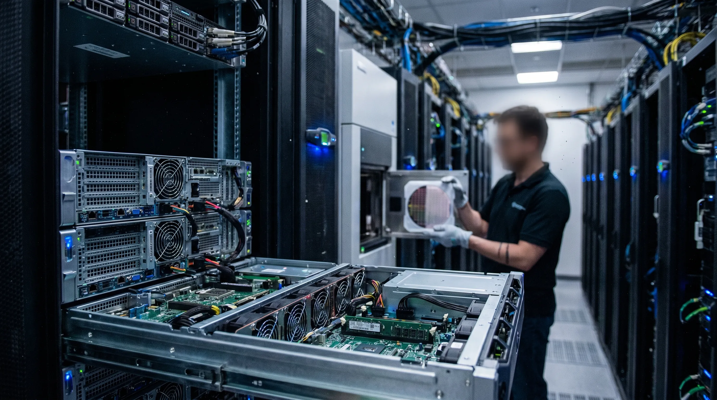
A gloved technician holds a silicon wafer in a data center aisle behind an open server chassis displaying internal components. © The GPU Trade Inc 2026
AMD said May 21, 2026 that its 6th‑generation EPYC server processor, codenamed “Venice,” has entered production ramp on TSMC’s 2nm (N2) process in Taiwan, with plans to expand manufacturing at TSMC’s Arizona facility.
The announcement marks the first public production ramp of a high‑performance server CPU on TSMC’s N2 node, a milestone for both AMD and the foundry as hyperscalers plan denser, more power‑efficient AI infrastructure.
AMD describes Venice as a Zen 6‑based EPYC family that can scale up to 256 cores per socket, positioning the chips for cloud, enterprise and AI/HPC workloads that favor many small cores and high memory throughput.
Early coverage of the ramp highlights AMD’s performance claims—some materials point to roughly a 70 percent performance uplift in targeted HPC workloads compared with prior generations, and AMD says Venice will deliver higher memory bandwidth for large models and data‑intensive simulations.
Packaging and system‑level changes are central to the Venice design. AMD plans EFB‑based 2.5D packaging and a new platform to support increased I/O, power delivery and memory channels needed for 256‑core sockets. The company also announced over $10 billion in Taiwan ecosystem investments to scale advanced packaging for next‑gen AI infrastructure.
TSMC’s N2 node uses gate‑all‑around nanosheet transistors and is the foundry’s first GAA process, which TSMC says improves efficiency and density for both mobile and larger AI/HPC chips. Qualifying a large server die like Venice on N2 suggests the node has reached maturity beyond smartphone SoCs.
The joint ramp in Taiwan, plus a stated follow‑on ramp in Arizona, reflects AMD’s effort to diversify supply and meet the volume needs of cloud customers, especially for regulated or domestic procurement requirements. Hyperscalers indicated interest in earlier briefings and AMD named cloud and AI as priority markets for Venice.
Server‑class dies are large and complex, so production ramps carry technical and logistical risk; yields, thermal characteristics and packaging throughput will determine how quickly Venice moves from wafer ramp to customer deployments. Analysts and foundry observers say the move reduces uncertainty about N2’s suitability for big datacenter chips but that volume scaling still needs monitoring.
The Venice ramp arrives as AMD holds a strong position in servers—coverage cites a record server CPU revenue share of roughly 46 percent in Q1 2026—giving the company leverage as it pitches higher core counts and energy efficiency to cloud customers.
For operators, the key attractions are denser compute per rack and better performance per watt for AI inference and training at scale, if AMD’s efficiency claims bear out in real deployments. That outcome depends on system design choices such as memory topology, cooling and power delivery for the new SP7‑class platforms that support Venice.
TSMC and AMD will be watched for two near‑term milestones: consistent N2 yields for large dies and the start of Arizona‑based volume production, which AMD says is planned but did not date precisely in its May announcement. Those milestones will shape delivery timelines for cloud customers and OEMs.
The Venice ramp is a notable inflection for datacenter silicon—if the chips reach volume at projected efficiency and throughput, enterprises and cloud providers could build denser AI and HPC clusters with smaller energy footprints. The immediate next step will be real‑world testing by hyperscalers and OEM validation across server ecosystems.