ASML Confirms Musk Talks on Terafab Megaproject
CEO says Elon Musk is “very serious”; raises supply, tech and geopolitical questions
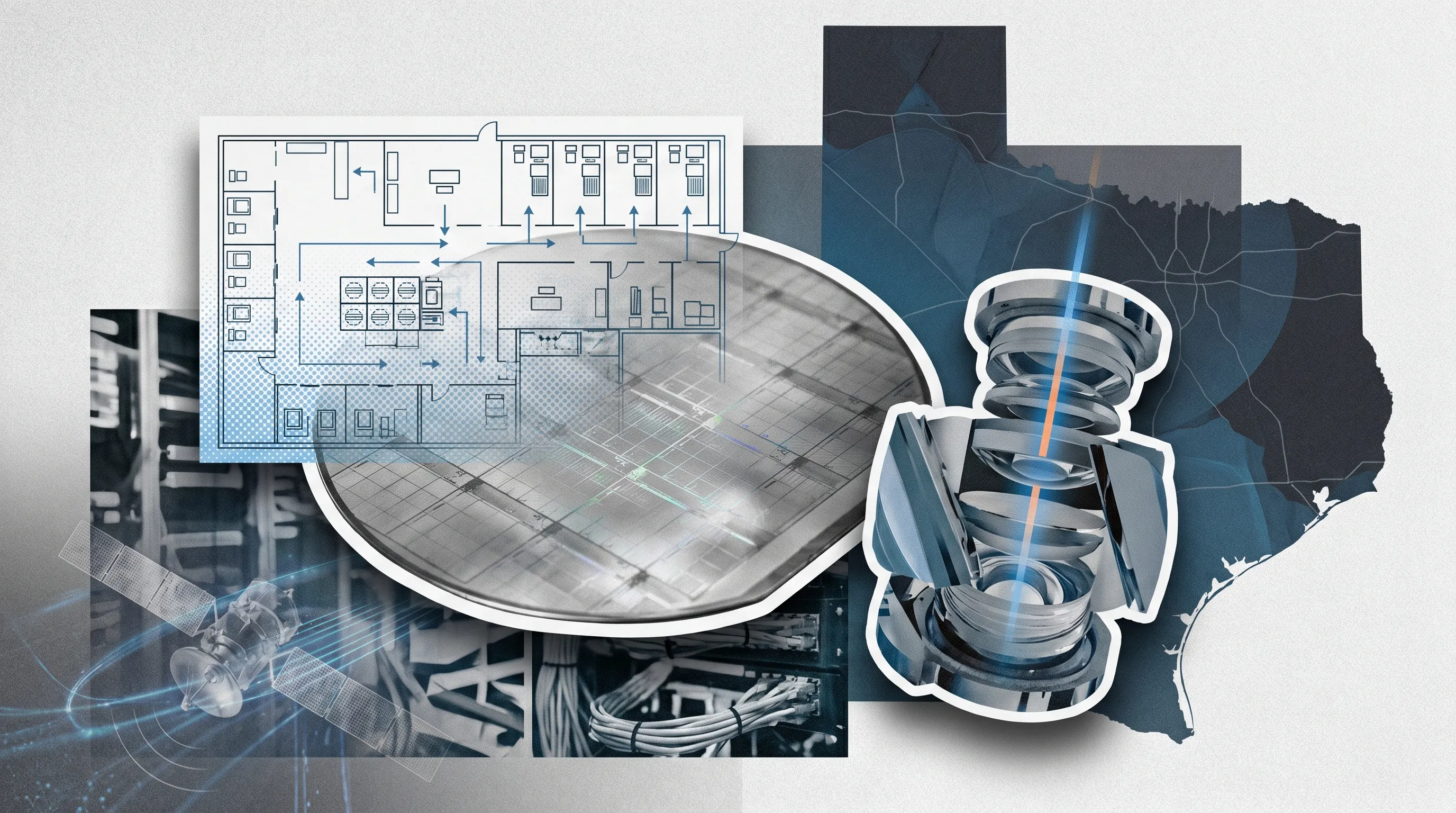
A composite graphic displays a silicon wafer, facility blueprints, optical equipment, satellite technology, and server infrastructure overlaid on a regional map. © The GPU Trade Inc 2026
ASML’s chief executive confirmed this week that he has spoken directly with Elon Musk about the proposed “Terafab” semiconductor megaproject, and described Musk as “very serious” about the plan.
The comment, made on the sidelines of a tech event in Antwerp, renewed scrutiny over the scale and implications of a privately led bid to build vast new chipmaking capacity in Texas.
Terafab was unveiled by Musk in March and has since ballooned in public estimates, with SpaceX filings and reporting showing an initial proposal of about $55 billion and potential total investment up to $119 billion if later phases proceed.
Musk and his companies have pitched Terafab as an integrated hub for logic chips, memory and advanced packaging to feed Tesla, xAI and SpaceX ambitions, and Intel has publicly signaled involvement to supply process technology such as its 14A node.
That prospect matters to ASML because its extreme ultraviolet (EUV) lithography systems are effectively mandatory for leading‑edge logic production, and the company says its tools are already in tight demand from established foundries and memory makers.
ASML’s CEO used the exchange to warn that global semiconductor capacity will be “tense” for the foreseeable future as AI, satellites and robotics drive demand, and he singled out projects such as Terafab and Starlink as potential stressors on equipment supply chains.
Industry analysts and reporters have highlighted tough practical limits for any new entrant attempting to build a full‑scale advanced‑node fab complex, noting that tool delivery rates, floor space, and the supply chain for parts and chemicals create multi‑year bottlenecks.
Energy, water and power distribution are also major complications for a Texas buildout of this size, with coverage flagging multi‑gigawatt power needs and local resource constraints that typical fabs must address through long‑term planning and infrastructure investment.
The revelation that Musk has held direct talks with ASML also feeds a broader geopolitical debate about how private mega‑projects could reshape global chip capacity and diplomatic leverage. Export controls on certain lithography platforms and proposed U.S. legislation such as the MATCH Act have already complicated equipment access for some customers, a point ASML’s CEO referenced when discussing market dynamics.
Supporters of Terafab argue that massive private investment could accelerate capacity expansion and reduce reliance on a handful of foundries, while critics say the project underestimates technical hurdles and could exacerbate shortages for other customers if it demands priority tool deliveries.
Executives at established chipmakers have publicly cautioned that building cutting‑edge fabs is “extremely hard,” and that securing the whole industrial ecosystem — from lithography to materials suppliers to qualified staff — is as important as capital. Comments from other industry leaders underscore why ASML and its machine backlog are central to any discussion about who can realistically scale advanced production.
For now, ASML’s confirmation of direct contact does not mean formal contracts or set orders for equipment, but it does signal that one of the few companies that can supply critical tools is treating Terafab as a serious potential customer. That recognition alone sharpens questions about timing, national policy, and whether private megaprojects can reshape the hardware foundation of future AI infrastructure.