Google Pushes TPUs Toward Million-Chip Scale
Trade reporting says power — not chips — is the limiting factor as fleets grow
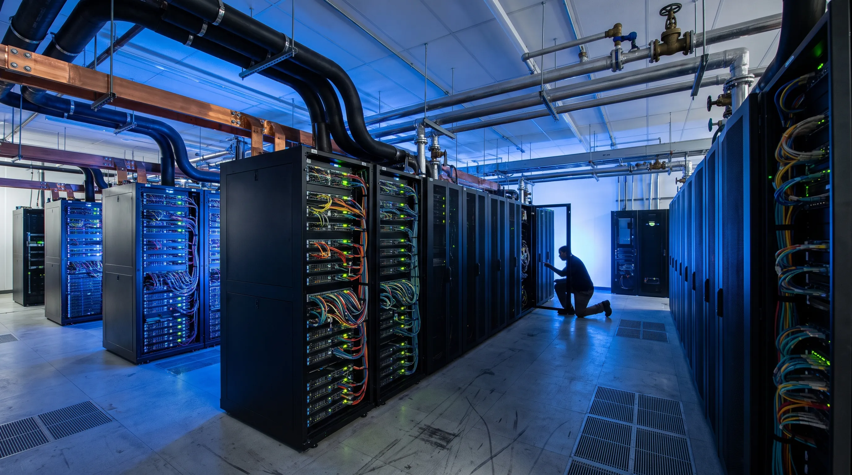
Trade reporting compiled Sept. 21–23, 2026 shows Google is moving aggressively to knit hundreds of thousands of Tensor Processing Units (TPUs) into single training clusters, even as power delivery and distribution increasingly shape how far those clusters can grow.
At Google Cloud Next in April, company engineers outlined an "AI Hypercomputer" architecture built around eighth‑generation TPUs — two chips, TPU 8t and TPU 8i — and said the stack can scale to more than one million chips across multiple data‑center sites. The blog post includes technical details about pod sizes, memory, and inter‑chip fabrics.
Google also described a new data‑center fabric called the Virgo Network and said a single data center could host roughly 134,000 TPUs in one fabric, while fabrics spanning multiple sites could link more than one million TPUs into a unified training cluster. Those system‑level claims are central to the trade coverage now flagging physical limits.
Industry trade coverage and follow‑up reporting note the same constraint in different words: once you build systems at the hundreds‑of‑thousands scale, the limiting variable shifts from silicon supply to how much conditioned power you can feed into racks, and how you distribute that power safely and efficiently across a campus. The reporting cites Google remarks at SEMICON Taiwan and analysis by trade outlets.
Customers of large AI clouds have already signed deals that assume gigawatts of TPU capacity. Public reports show Anthropic and some other model builders negotiating access to up to a million Google chips — deals that would bring more than a gigawatt of accelerator capacity online in 2026 if fully provisioned. Those commercial arrangements underline why power planning has moved from theoretical risk to operational reality.
That commercial interest collides with supply‑chain and packaging choices. Google’s own materials highlight how TPU 8i expands on‑chip SRAM and high‑bandwidth memory to host large KV caches, but those memory and power density improvements increase per‑rack electrical and thermal demands. Analysts say choices about HBM generation, chip form factors, and module packaging all change how much current a rack will draw.
Power delivery is not just raw megawatts. Hyperscalers must rethink busbars, PDUs, switchgear, and on‑site substations when a campus grows toward multi‑gigawatt consumption. Industry infrastructure reports say hyperscalers are front‑loading physical facility spending and that grid access, transformer capacity, and local permitting are becoming gating factors for expansion.
Cooling and heat rejection follow electrical limits. Moving to higher chip counts and denser rack power draws is pushing adopters toward liquid cooling and closer integration between server packaging and building HVAC, according to equipment trackers and vendor roadmaps. Those choices make deployments more efficient but also more complex to build and operate.
For suppliers, the tension is twofold. Foundries and memory makers may be able to ramp wafer capacity, but that does not immediately translate to usable cluster capacity if the data‑center cannot accept the extra load. Conversely, building more facility power without matching chip availability risks underutilized megawatts. Several market trackers now flag this mismatch as a coordination problem across chip design, packaging, and data‑center planning.
Some hyperscalers have taken different approaches. Amazon’s Trainium rollouts and multi‑site GPU architectures show that you can scale large pools of accelerators if you stitch capacity across geographically diverse sites with staggered power footprints. Google’s strategy instead leans on tighter vertical integration — custom chips, co‑designed networks, and dense fabrics — which concentrates the power problem but can yield better utilization if the power side is solved.
The practical consequences are immediate: project timelines stretch, regional buildouts get prioritized based on grid access, and deals that assume elastic capacity may come with more complex clauses around power availability and phased ramp‑ups. Trade coverage this week emphasizes that the next frontier in AI compute may be the transformer and the transformer substation, not only the transformer neural network.
Scaling TPUs toward million‑chip fleets remains technically feasible but operationally constrained. The current reporting paints a picture of competing shortages — of chips, of qualified packaging and assembly, and increasingly of power and cooling capacity — and signals that successful large‑scale deployments will require close coordination between chip designers, server packagers, data‑center planners, and utilities.