Google readies TPU 8t/8i as hyperscalers diversify AI silicon
Google splits TPU v8 for training and inference as clouds mix custom ASICs and GPUs
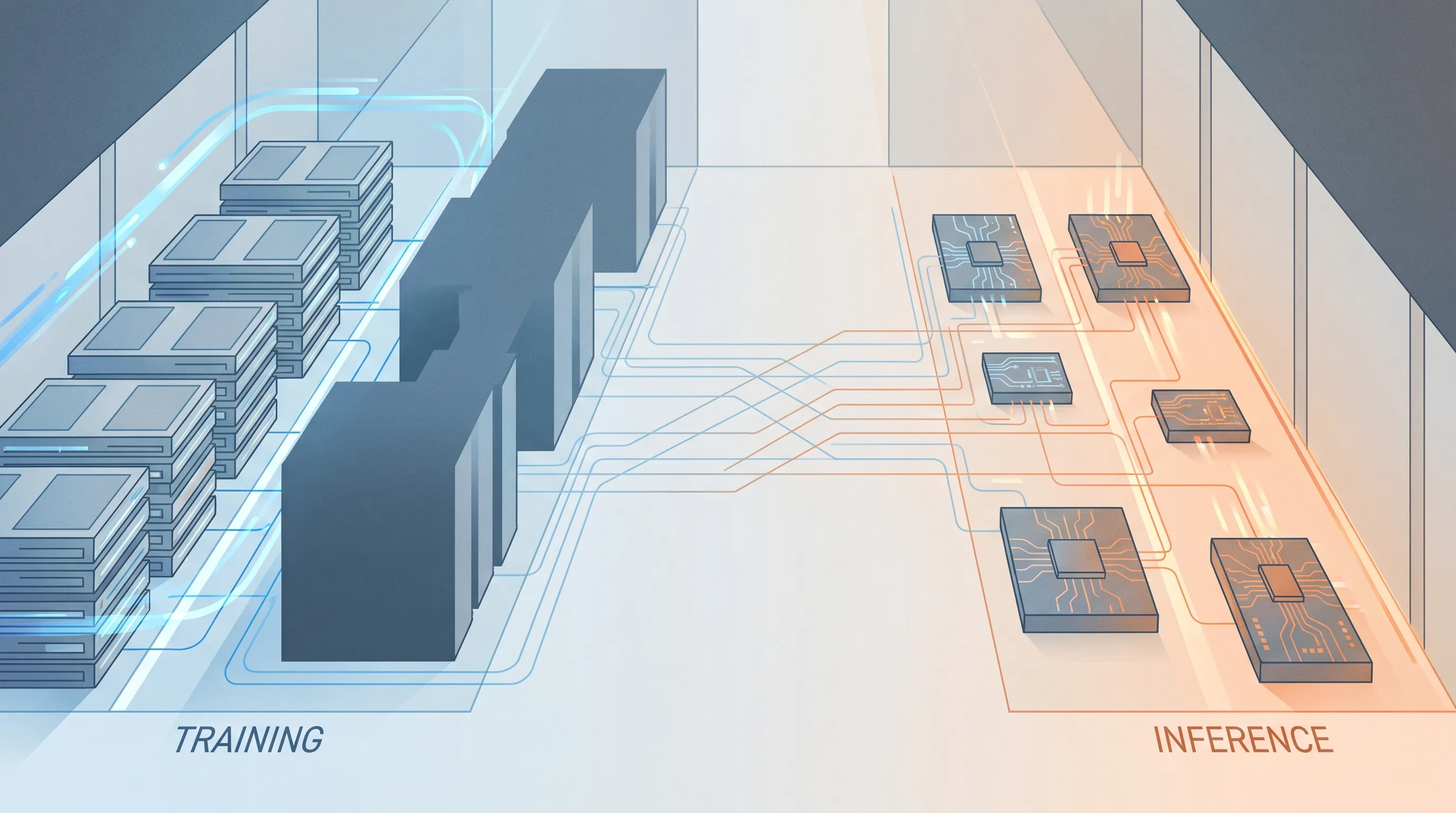
Google Cloud this spring unveiled an eighth generation of Tensor Processing Units and, for the first time, split the design into a training chip (TPU 8t) and an inference chip (TPU 8i).
The split is concrete: Google describes TPU 8t as a training-focused part that scales to very large superpods and TPU 8i as an inference-optimized design with much larger on‑chip SRAM to host key‑value caches for long contexts.
On paper the numbers are striking — Google and independent reporting show an 8t superpod design that can scale to thousands of chips and deliver multi‑exaflop FP4 throughput, while 8i clusters use denser, lower‑latency groupings tailored for real‑time agentic workloads.
Google framed the effort as infrastructure tuned for an “agentic” era of AI — systems that run persistent, multi‑step reasoning and fast recall across long contexts — and said the new TPUs pair with new fabric and host CPU designs to meet those demands.
The rollout follows a staged approach rather than instant global availability: Google’s v7 Ironwood family is already being phased into certain zones, and v8 capacity will appear similarly by region as operators validate power, cooling, and networking.
The v8 training/inference split also fits a wider industry pattern: hyperscalers are diversifying away from an all‑GPU model and building or buying specialized ASICs to control cost and capacity. That trend shows up in public cloud offerings and supply deals across the sector.
Economics are the clearest short‑term driver: Google and others argue TPU 8i delivers much better performance‑per‑dollar for inference at scale, while TPU 8t raises training efficiency and pod‑level throughput — both levers that change the per‑token and per‑training‑step math customers use to compare clouds.
But the hardware is only half the work. TPUs use different software stacks and preferred frameworks — JAX on Google Cloud is a leading example — and porting models from GPU ecosystems to TPU pipelines requires engineering, testing, and often model tuning. That friction matters for enterprise migration decisions.
The new designs also force data‑center changes: denser TPUs and larger superpods drive liquid cooling, higher‑capacity power delivery, and faster fabric topologies that Google labeled in presentations as part of its Virgo/Boardfly networking story. Operators balancing rack density and regional constraints will choose where to place TPU clusters carefully.
Hyperscaler customers are already reacting. Large AI firms and cloud tenants have been signing capacity agreements and experimenting with TPU fleets, and some customers that previously ran primarily on GPUs are testing TPUs for parts of their pipelines where price or latency gains are clear.
For cloud operators the practical choice is increasingly about mixing silicon instead of choosing only one vendor. That makes pricing and consumption models more complex, but it can also create negotiating leverage for large customers and new business lines for providers offering multi‑accelerator portfolios.
For enterprise buyers the immediate takeaway is pragmatic: benchmark real workloads, insist on portability and clear pricing for long contexts or agentic flows, and plan procurement to avoid single‑vendor lock‑in as hyperscalers roll out heterogeneous silicon and regional capacity.