SK hynix Tests Intel EMIB, Shares Jump
May 11 reports say SK hynix is evaluating Intel's 2.5D EMIB to link HBM and logic dies
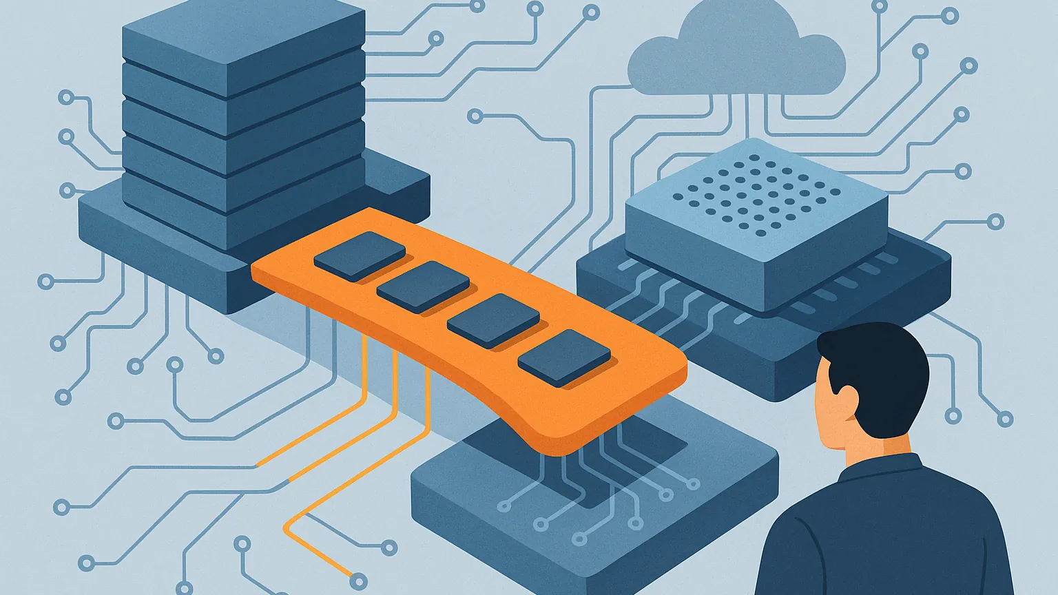
An illustration depicts a person observing an orange hardware component connecting a server rack to a computer processor. © The GPU Trade Inc 2026
Reports that SK hynix is testing Intel’s 2.5D EMIB (Embedded Multi‑die Interconnect Bridge) to integrate high‑bandwidth memory (HBM) with logic dies surfaced on May 11, 2026, prompting a sharp investor reaction.
After the reports, SK hynix’s shares climbed to record levels on South Korean markets, with traders citing the packaging news as a catalyst for optimism about the company’s role in the AI supply chain.
EMIB is a 2.5D packaging method Intel has used to link multiple dies on a substrate without a full silicon interposer. It offers a different take from TSMC’s CoWoS and from hybrid bonding approaches that are gaining traction for next‑generation HBM.
For AI accelerators, how HBM is attached to compute dies matters as much as raw DRAM capacity. Packaging affects latency, power, thermal behavior and manufacturing throughput — all crucial to hyperscalers and chip designers chasing higher performance per watt.
A key driver behind interest in an EMIB route is capacity pressure at established packaging nodes. Industry reporting has highlighted tightness around TSMC’s CoWoS capacity and rising lead times for advanced interposer services, giving memory makers incentives to explore alternatives.
SK hynix already occupies a dominant position in the HBM market and has been investing heavily to expand output for AI customers. The company’s recent capital plans and orders for advanced lithography tools underline a broader push to scale HBM supply.
Technically, EMIB and hybrid bonding are different. Hybrid bonding (fluxless or direct bonding) promises tighter die‑to‑die connections and is touted for future HBM4/16‑high stacks, while EMIB can be faster to deploy as a substrate‑level bridge between pre‑tested dies. Each approach carries tradeoffs in yield, cost and thermal routing.
If SK hynix moves from testing to volume production of EMIB‑coupled HBM, chip companies and hyperscalers would gain another packaging pathway. That could loosen reliance on specific foundry packaging services and give OEMs more latitude when specifying memory‑logic pairings for next‑generation accelerators.
The reports did not include direct confirmations from SK hynix or Intel at the time they appeared, and analysts caution that testing is an early stage that may not lead to large‑scale adoption without yield and supply validation. Companies often evaluate multiple packaging routes in parallel.
Intel has been promoting EMIB and next‑generation EMIB‑T variants as part of its packaging playbook, and trade reporting suggests the company hopes to expand EMIB’s use beyond its own logic dies into broader industry supply. Any practical rollout would require qualifying substrate suppliers and proving consistent yields at scale.
For investors and customers, the near‑term significance is clear: alternative packaging experiments like this can influence procurement strategies, pricing leverage and timelines for accelerator launches. The longer‑term outcome depends on technical results, commercial agreements between SK hynix, Intel and potential foundry or platform partners, and how quickly customers embrace a new assembly route.